
Voltage Source Inverter (VSI) is a type of converter that converts DC voltage to AC voltage. It is also known as voltage-fed inverter (VFI). A VSI consists of a DC power source, transistors (thyristors, IGBT, MOSFET, etc.) for switching, and a DC link capacitor (to provide filtering and minimize fluctuations). An ideal VSI keeps the voltage constant throughout the process.
The DC input source can be batteries stacked in series or parallel, photovoltaic cells, or rectified output from another AC power source. It can be used in both single phase and three phase topologies.
You are viewing: What Is Vsi
Voltage Source Inverter can operate in two modes:
- Square wave mode.
- PWM (Pulse width modulation) mode.
Voltage source inverter is available in three configurations – single-phase half-bridge, single-phase full-bridge, and three phase. Single phase voltage source inverters are ideally used in high power supplies, active filters, and single-phase UPS applications whereas three phase voltage source inverters are used in adjustable speed drives (ASDs), UPS, flexible AC transmission systems (FACTS) devices such as the STATCOM, and PV generators.
Single Phase Half-Bridge Voltage Source Inverter
The circuit diagram of a single-phase HB-VSI with a load is shown below
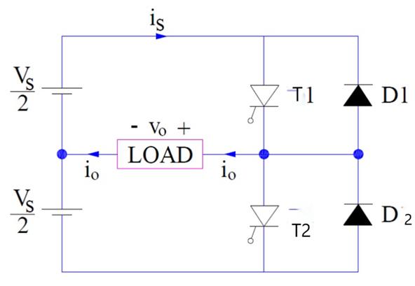
In this type of topology, one thyristor T1 conducts for half of the time period and the other thyristor T2 conducts for the other half of the time period of the output waveform. The diodes are connected anti-parallel with the thyristor and will allow the current to flow when the main thyristor is turned off. Diode D1 will conduct when the voltage is positive and the current is negative, and diode D2 will conduct when the voltage is negative, and the current is positive. It is especially useful in the case of non-resistive loads. When the diode conducts, the energy is fed back to the DC source and hence, these diodes (D1 & D2) are called flyback diodes.
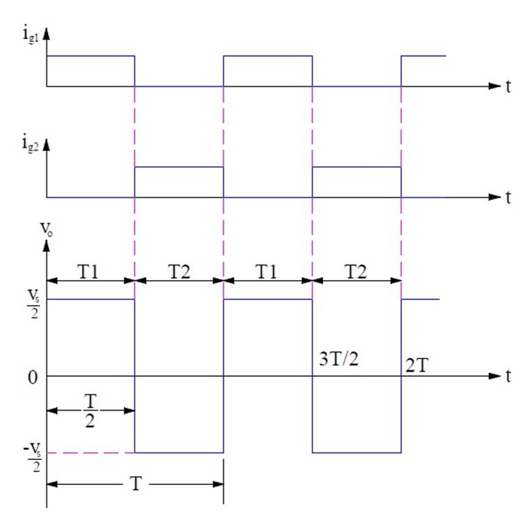
Each thyristor is triggered via its gate. While analyzing the circuit, it is assumed that each thyristor conducts for the duration its gate pulse is present and is commutated as soon as this pulse is removed. The gating signal for thyristor T1 (ig1) and thyristor T2 (ig2) and the output voltage waveform of this inverter are shown below.
Read more : What Is The Difference Between Baptist And Methodist Religion
It can be observed that ig1 is applied for a period of 0 <t≤ (T/2), the thyristor T1 conducts during this period and the load is directly connected to the source Vs/2 on the upper arm of the circuit and the output voltage equals Vs/2 during this time. ig1 is removed at time T/2, thyristor T1 gets turned off, ig2 is applied and thyristor T2 starts conducting. The load is then connected directly to the -Vs/2 on the lower arm (it has the opposite polarity as compared to the upper arm). The output voltage is now -Vs/2 as shown in the waveform above.
The resulting output waveform is an alternating square wave with a frequency of 1/T Hz and an amplitude of Vs/2. The frequency is controlled by changing the value of the period, T.
The main drawback of this topology is its requirement for a 3-wire DC source. The output is also half the magnitude of the input voltage which can be seen as a drawback. These drawbacks are however overcome in the full-bridge topology.
Single Phase Full-Bridge Voltage Source Inverter
The circuit diagram of a single-phase FB-VSI with a load is shown below:
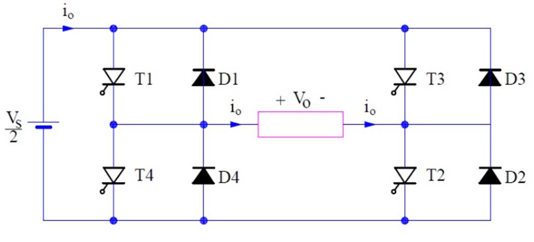
This topology consists of 4 thyristors, T1-T4, 4 diodes D1-D4, a 2-wire DC source, and a load. The diodes are connected antiparallel to the thyristors, and they allow the current to flow when the main thyristor is turned off. When these diode conduct, the energy is fed back to the DC source and hence, these diodes (D1 to D4) are called flyback diodes. It is assumed that each of the thyristors only conducts for the period its gate signal is present and as soon as the gate signal is removed, the thyristors get turned OFF.
The thyristors are triggered diagonally. for half of the time period, thyristors T3 & T4 will be ON while for the remaining half of the time period, T1 & T2 will be ON. Only two thyristors are turned ON in half of the period. The thyristors turn on in a sequence as shown below:
- For the time 0 <t≤ (T/2), thyristors T1 & T2 conduct and load voltage Vo = Vs.
- For the time (T/2) <t≤ T, thyristors T3 & T4 conduct and load voltage Vo = -Vs.
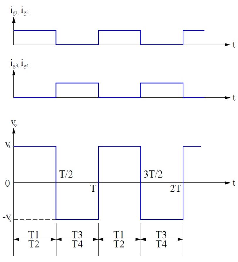
The gate signal and the output voltage waveforms are shown below:
Read more : What Is 85 Of 20
The thyristors T1 & T2 are triggered simultaneously for a time T/2. Therefore, the load is connected to the source through T1 & T2, and hence, the load voltage is equal to the source voltage with positive polarity. As soon as the gate signal (ig1 & ig2) are removed, T1 and T2 gest are turned OFF. However, at the same instant gate signal (ig3 & ig4) are applied and hence, T3 & T4 are turned ON. When T3 & T4 are conducting, the load gets connected to the source. The load voltage magnitude is again Vs but with reverse polarity.
3-Phase Voltage Source Inverter
This VSI is a 6-step bridge inverter. It consists of a minimum of six thyristors or IGBTs. In inverter terminology, a step is defined as a change in the firing from one thyristor to the next thyristor in a proper sequence. For getting one cycle of 360°, each step is of 60° interval. This means thyristors will be gated at a regular interval of 60° in a proper sequence so that three-phase AC output voltage is synthesized at its output. The circuit diagram of a 3-phase VSI is shown below:
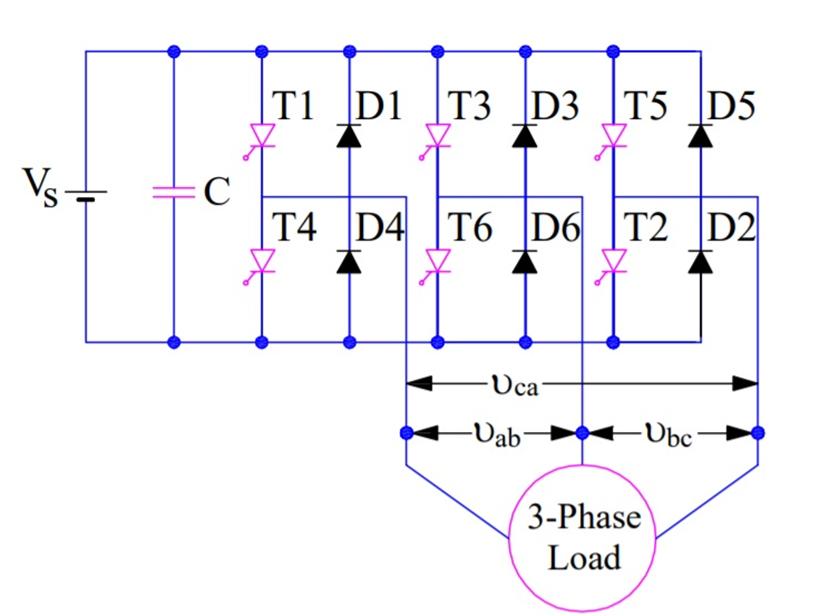
The numbering of the thyristors is done in the order in which they are triggered. It can also be observed that 3-phase VSI is equivalent to 3 half-bridge inverters put side by side and the load is assumed to be star connected. This inverter works in two modes, 180̊ conduction mode (each thyristor conducts for 180°)and 120̊ conduction mode (each thyristor conducts for 120°). In both cases, gate signals are applied and removed at 60̊ intervals. For this article, the 180̊ conduction mode is explained.
For the 180° conduction mode, the triggering occurs in the following sequence:
- Step-I: In step-I, thyristors T1, T6, and T5 conduct.
- Step-II: T1, T2 and T6 conducts. Mind that T5 is turned off.
- Step III: Now, will have to turn off T6. Therefore, this step will comprise of conduction of thyristors T1, T2, and T3.
- Step-IV: This time, T1 has to be turned off, and hence, T2, T,3, and T4 shall conduct this step.
- Step-V: T4, T3, and T5 conduct,t, and T2 are turned off.
- Step VI: T4, T6, and T5 conduct, and T3 is turned off.
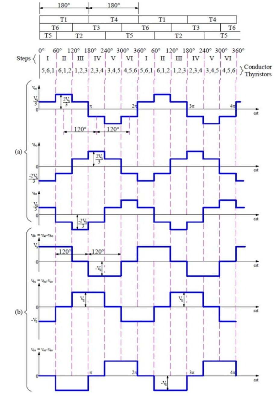
For each cycle of the output voltage of each phase, six steps are required and each step has a duration of 60°.
The line voltage Vab = Vao + Vbo or Vab = Vao – Vbo is obtained by reversing Vbo and adding it to Vao. This is shown in the output waveform (b). Similarly, line voltages Vbc & Vca are plotted.
While the VSI offers multiple advantages such as small size, the output voltage is independent of the type of load, etc there are some disadvantages as well. Short circuits in case of failure in not preventable for VSI. The switching frequency is also low, up to 500 Hz. The input power factor is low (<1) which leads to reactive power loss.
Click here to learn more about DC-AC Inverters featured on everything PE.
Source: https://t-tees.com
Category: WHAT